
Feature
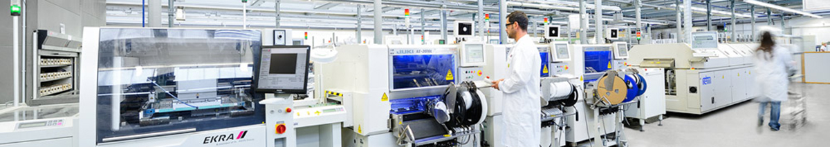
Flying probe testers are used to test circuit boards and are divided into two categories: one is to test PCBs, and the other is to test PCBAs.
The flying probe tester for testing PCBs is an instrument for testing PCBs (printed circuit boards) with high-density component layout, many layers, high wiring density, and small test point distance. It mainly tests the insulation and conduction values of the circuit board. The tester generally adopts the "true value comparison positioning method" to monitor the test process and fault points in real time to ensure the accuracy of the test.
The flying probe tester for testing PCBA mainly performs electrical tests on the values and electrical characteristics of electronic components;
The flying probe tester has the characteristics of fine pitch, no grid restrictions, flexible testing, and fast speed.
Detail Image
Specifications
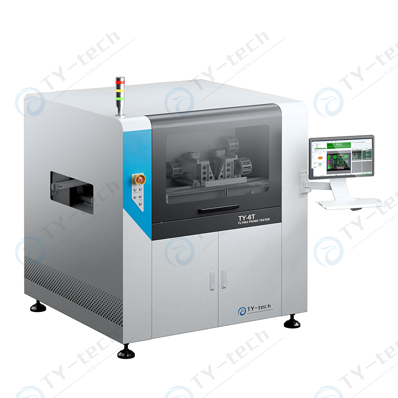
| Model | TY-6T | |
|
Main Spec
|
Minimum Chip
|
0201(0.8mm x 0.4mm)
|
|
Min Compenent Pin Spacing
|
0.2mm
|
|
|
Min Contact Pad
|
0.15mm
|
|
|
Probes
|
4 Heads(Top)+2 Heads(Bottom)
|
|
|
Probe elastic force
|
120g(Default)
|
|
|
Probe Rated Stroke
|
1.5mm
|
|
|
Testable point types
|
Test points, Pads, Device Dlectrodes
Connectors, Irregular Components
|
|
|
Testing speed
|
Max 17 Steps/Sec
|
|
|
Repeatability
|
±0.02mm
|
|
|
Belt high
|
900±20mm
|
|
|
Belt Wideth
|
50mm ~ 410mm
|
|
|
Track width adjustment
|
Auto
|
|
|
Inline Mode
Offline Mode
|
Left (Right) In , Right (Left) Out
Left In, Left Out
|
|
|
Optics
|
Camera
|
2 Colorful Cameras, 12M Pixels
|
|
Laser Displacement Sensor
|
2 Sets
|
|
|
Test Area
|
Max Test Area
|
500mm x 410mm
|
|
Min Test Area
|
60mm x 50mm
|
|
|
TOP Clearence
|
≤60mm
|
|
|
BOT Clearence
|
≤60mm
|
|
|
Board Edge
|
≥3mm
|
|
|
Thickness
|
0.6mm ~ 6mm
|
|
|
Max PCBA Weight
|
5kg
|
|
|
Motion
Parameters
|
Probe Return Height
|
Programmed
|
|
Probe Pressing Depth
|
Programmed
|
|
|
Probe Soft Landing
|
Programmed
|
|
|
Z Distance
|
-3mm ~ 70mm
|
|
|
XY / Z Acceration
|
Max 3G / Max 20G
|
|
|
XY Driver
|
Ballscrew
|
|
|
XYZ Measure
|
/
|
|
|
XY Lead Rail
|
P-Grade precision guide rail
|
|
|
Testing
Capability
|
Resistors
|
10mΩ ~ 1GΩ
|
|
Capacitors
|
10pF ~ 1F
|
|
|
Inductors
|
10uH ~ 1H
|
|
|
Diodes
|
Yes
|
|
|
Zener diode
|
40V
|
|
|
BJT
|
Yes
|
|
|
Relay
|
40V
|
|
|
FETs
|
Yes
|
|
|
DC Constant Current Source
|
100nA ~ 200mA
|
|
|
DC Constant Voltage Source
|
0 ~ 40V
|
|
|
AC Constant Current Source
|
100 ~ 500mVrms(200hz ~ 1Mhz)
|
|
|
Panel Test
|
Yes
|
|
|
2D Barcode
|
Yes
|
|
|
PCBA Deformation Compensation
|
Yes
|
|
|
MES Connection
|
Yes
|
|
|
LED Testing
|
Option
|
|
|
Open Pin
|
Option
|
|
|
On board programing
|
Option
|
|
|
Vayo DFT (6 CAD)
|
Option
|
|


