
Feature
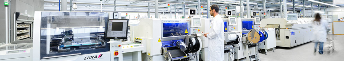
A flying probe tester is a system for testing PCBs in a manufacturing environment. Instead of using the traditional bed-of-nails interface found on conventional in-circuit testers, flying probe testing uses four to eight independently controlled probes that move to the component under test. The unit under test (UUT) is transported to the tester via a belt or other UUT transport system. Then secured, the tester's probes contact the test pads and vias to test individual components of the UUT. The test probes are connected to drivers (signal generators, power supplies, etc.) and sensors (digital multimeters, frequency counters, etc.) through a multiplexing system to test components on the UUT. While one component is being tested, other components on the UUT are electrically shielded by the probes to prevent interference with the readings.
【Key Features】
① Six probes on double side with best price
② High accuracy ( 01005 package supported )
③ Precision linear rail system with high re-positioning accuracy
④ Online / Inline transmission supported
⑤ Horizonal transmission
⑥ Static LCRD test supported
Detail Image
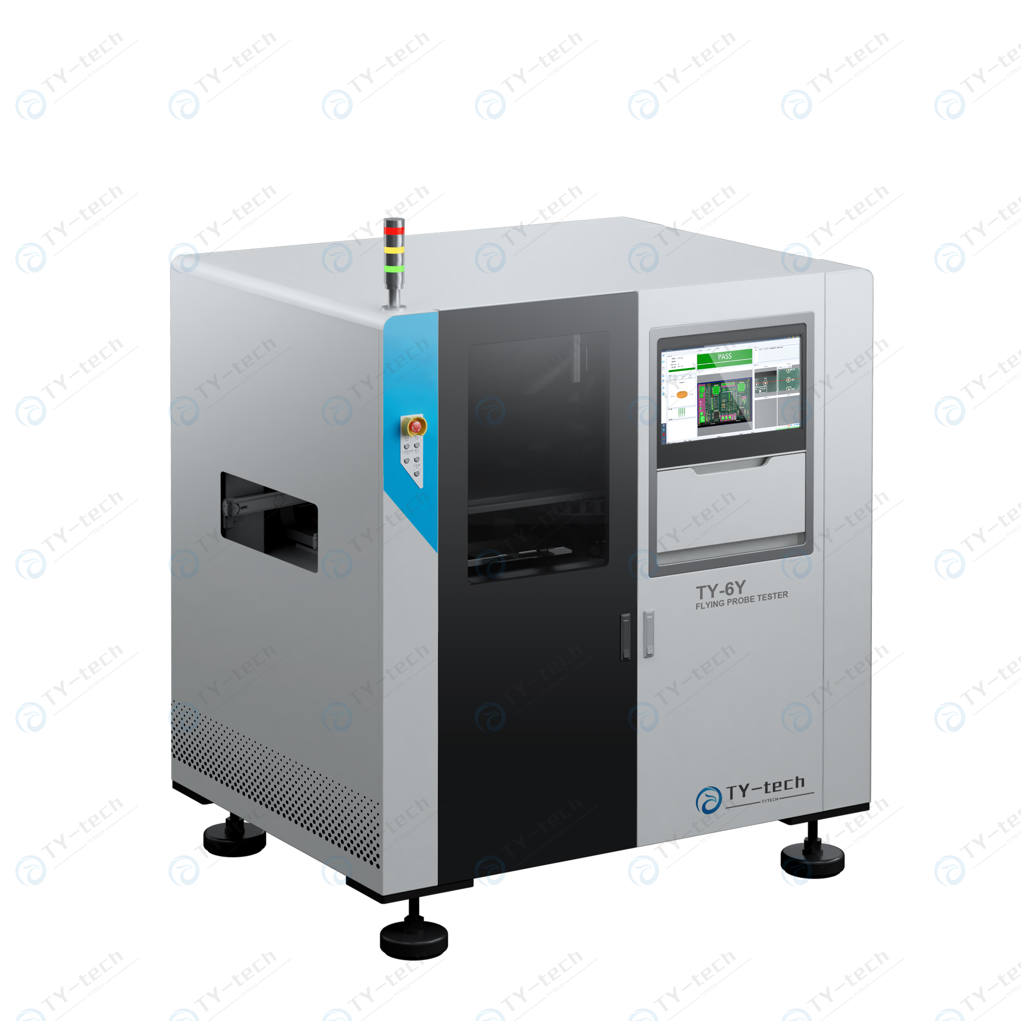
Specifications
| Model | TY-6Y | |
|
Main Spec
|
Minimum Chip
|
01005(0.4mm x 0.2mm)
|
|
Min Compenent Pin Spacing
|
0.2mm
|
|
|
Min Contact Pad
|
0.15mm
|
|
|
Probes
|
4 Heads(Top)+2 Heads(Bottom)
|
|
|
Probe elastic force
|
120g(Default)
|
|
|
Probe Rated Stroke
|
1.5mm
|
|
|
Testable point types
|
Test points, Pads, Device Dlectrodes
Connectors, Irregular Components
|
|
|
Testing speed
|
Max 20 Steps/Sec
|
|
|
Repeatability
|
±0.005mm
|
|
|
Belt high
|
900±20mm
|
|
|
Belt Wideth
|
50mm ~ 630mm
|
|
|
Track width adjustment
|
Auto
|
|
|
Inline Mode
Offline Mode
|
Left (Right) In , Right (Left) Out
Left In, Left Out
|
|
|
Optics
|
Camera
|
4 Colorful Cameras, 12M Pixels
|
|
Laser Displacement Sensor
|
4 Sets
|
|
|
Test Area
|
Max Test Area
|
640mm x 600mm
|
|
Min Test Area
|
50mm x 50mm
|
|
|
TOP Clearence
|
≤50mm
|
|
|
BOT Clearence
|
≤50mm
|
|
|
Board Edge
|
≥3mm
|
|
|
Thickness
|
0.6mm ~ 6mm
|
|
|
Max PCBA Weight
|
5kg ( 10kg Option )
|
|
|
Motion
Parameters
|
Probe Return Height
|
Programmed
|
|
Probe Pressing Depth
|
Programmed
|
|
|
Probe Soft Landing
|
Programmed
|
|
|
Z Distance
|
-3mm ~ 53mm
|
|
|
XY / Z Acceration
|
Max 3G / Max 20G
|
|
|
XYZ Driver
|
Linear Motor
|
|
|
XYZ Measure
|
Linear scale
|
|
|
XY Lead Rail
|
P-Grade precision guide rail
|
|
|
Testing
Capability
|
Resistors
|
10mΩ ~ 1GΩ
|
|
Capacitors
|
10pF ~ 1F
|
|
|
Inductors
|
10uH ~ 1H
|
|
|
Diodes
|
Yes
|
|
|
Zener diode
|
40V
|
|
|
BJT
|
Yes
|
|
|
Relay
|
40V
|
|
|
FETs
|
Yes
|
|
|
DC Constant Current Source
|
100nA ~ 200mA
|
|
|
DC Constant Voltage Source
|
0 ~ 40V
|
|
|
AC Constant Current Source
|
100 ~ 500mVrms(200hz ~ 1Mhz)
|
|
|
Panel Test
|
Yes
|
|
|
2D Barcode
|
Yes
|
|
|
PCBA Deformation Compensation
|
Yes
|
|
|
MES Connection
|
Yes
|
|
|
LED Testing
|
Option
|
|
|
Open Pin
|
Option
|
|
|
On board programing
|
Option
|
|
|
Vayo DFT (6 CAD)
|
Option
|
|


