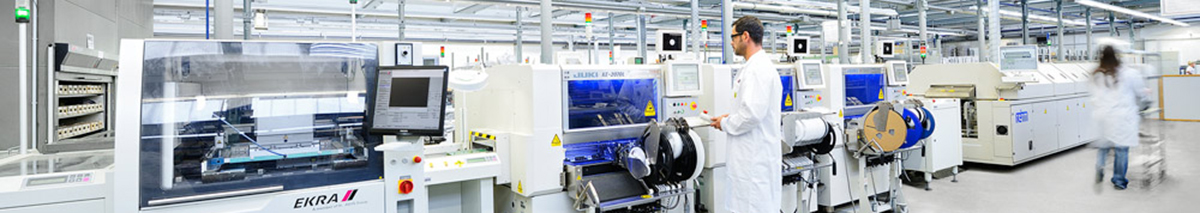
Wave soldering is a common soldering technology, mainly used in mass production of circuit boards. In the wave soldering process, “bridging” is a common problem, which refers to the appearance of solder connection between two or more solder joints that should not be connected, resulting in a short circuit. Bridging can be caused by a variety of reasons, and the following are some of the main reasons and corresponding solutions:[/prisna-wp-translate-show-hide
Causes of wave soldering tinning:
1. The solder temperature is too high: high temperature will increase the fluidity of the solder and easily form tinning.
2. Insufficient preheating: If the PCB is not preheated sufficiently, the temperature of the pad and component feet will be lower than the solder temperature, resulting in excessive solder flow.
3. Too much flux or poor quality: excessive flux or low-quality flux will increase the fluidity of the solder and easily form tinning.
4. Improper wave crest height: too high wave crest will increase the solder contact area and increase the risk of tinning.
5. Unreasonable pad design: such as too small pad spacing, pad shape is not suitable for automatic soldering, etc.
6. Inaccurate component placement: the component foot deviates from the center of the pad, causing the solder to flow to the wrong position when cooling.
7. Impurities in the solder: impurities in the solder will affect its fluidity and adhesion, resulting in tinning.
Solution to wave soldering with tin:
1. Adjust the solder temperature: Make sure the solder temperature is within the appropriate range and avoid being too high.
2. Optimize the preheating process: Ensure that the PCB is fully preheated so that the entire welding area reaches a consistent temperature.
3. Control the use of flux: Use an appropriate amount of high-quality flux, and adjust the amount of flux sprayed if necessary.
4. Adjust the wave crest height: Adjust the wave crest height to a suitable range to reduce unnecessary solder contact.
5. Improve pad design: Ensure pad spacing, shape and size are suitable for automatic welding processes.
6. Improve component positioning accuracy: Use more precise component placement equipment to ensure that component pins are accurately aligned with the pads.
7. Regular cleaning and maintenance: Keep the solder tank clean, remove impurities, and ensure solder quality.
Through the above measures, the risk of tin connection during wave soldering can be significantly reduced. In actual operations, it may be necessary to combine multiple methods to solve problems based on specific circumstances.
Post time: Sep-26-2024


